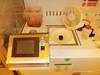
Nano-Bio
 |
|
 |
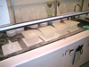
| Multiplex Assays, FlashGel Electrophoresis, PCR Thermal Cycling, Cell Culturing/Incubation, Glove Box, Chilled Work Space, Freeze Drying, Autoclave, Centrifuge, Cell Counting |
|
Resist Processing Spin & Spray
 |
|
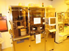 |
| OiR 620-7i, S1800 Series, SPR220 Series, SPR700 Series, SPR955CM, STR1045/1075, ARC, UV210, AZ9260, AZ nLOF, SU8, Polyimide, BCB, KMPR, LOR, ProTEK SR25 & Others |
|
Dry Etching
 |
|
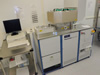 |
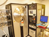
| RIE, ICP and DRIE using: CHF3O2, CHF3Ar, CF4, SF6O2, SF6C4F8, Cl2, BCl3, XeF2 and Others with Full Control over RF/ICP Power, Chamber Pressure, Temperature and Gas Flowrates |
|
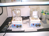
Wet Etching/Chemistry
 |
|
 |
| KOH, TMAH, HF, BOE, Gold Etch, Aluminum Etch, Copper Etch, Chrome Etch, Titanium Etch, Pad Etch, Aqua Regia, HCL, Nitric, Sulfuric, Phosphoric, Hot Piranha, Hot Nanostrip and Others |
|
Thin Film Deposition
 |
|
 |
| Evaporation (Ebeam, Thermal), Sputter Deposition (DC& RF), PECVD, Atomic Layer Deposition, Molecular Vapor Deposition, Pulsed Laser Deposition, Conductive Polymer Vapor Deposition |
|
Test & Metrology
 |
|
 |
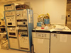
| Stress, PH, Thickness, Refractive Index, Transmission,/Absorption/Reflection, Step Height, Surface Roughness, Contact Angle, Viscosity, ZetaPotential, Resistivity, Molecular Weight, FTIR |
|
Furnace Processing
 |
|
 |
| Thermal Oxidation (Wet & Dry), LPCVD Nitride, LTO and HTO,
Poly-Silicon, Annealing (All Types), Doping (Boron, Phosphorus & POCl3) |
|
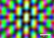
Microscopy
 |
|
 |
| Dark Field, Bright Field, Inverted, Polarized Light, Stereoscopic, DIC, Confocal, Fluorescence, TIRF, AFM, SEM and STEM including Sample Prep (Cutting, Polishing, Coating, Staining) |
|
Mask Layout/Design/Exposure
 |
|
 |
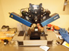
| CAD Layout & Design(Multiple Levels with Alignment Marks, Verniers, Test Structures, etc), Mask Exposure (Laser Writer & Pattern Generator), Mask Develop/Etch/Strip |
|
Wafer Bonding
 |
|
 |
| Cleaning (RCA) & Surface Activation, Fusion Bonding, Adhesive Bonding, Anodic Bonding, Eutectic Bonding, Water Bonding, Furnace
Annealing, Bond Strength Testing & Other |
|
Ion Implantation & Activation
 |
|
 |
| Implantation Screening, Ion Implantation (with Arsine, Phosphine, Boron Trifluoride, Carbon Dioxide, Argon & Helium sources), Thermal Activation (Furnace, RTA & RTP) |
|
Lithography:Contact & Stepper
 |
|
 |
| Contact Aligners (MA6, EV620 and ABM), Optical Steppers (i-Line &
g-Line), Deep UV Stepper (ASML), Whole Wafers, Chips, Temporary Handle Wafers All Possible |
|
Other Services
 |
|
 |
| Electroplating (Au, Cu, Ni and Other), Critical Point Drying, IV Probe Station, Zyvex NanoProbe Station, Wire Bonding, Soft Lithography (PDMS Casting and Bonding), Parylene, Nanoimprint &Other |
|
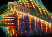
Carbon Nanotubes & Graphene
 |
|
 |
| First Nano ET3000 Carbon Nanotube/Graphene Furnace with Hydrogen and Methane Ambient (Samples up to 100mm Diameter), Manual Tube Furnace, Seed Liftoff |
|
Electron Beam Lithography
 |
|
 |
| JEOL6300 and JEOL9300 Ebeam Lithography Systems using PMMA, MMA, ZEP520A, ZEP7000, NEB 31A3, ma-N 2403, XR1541 (HSQ), UV56,
UVN30 and Others, Bilayer & Trilayer |
|
Dicing, Drilling, Milling &Other
 |
|
 |
| Wafer Dicing, Chemical Mechanical Polishing, Diamond Film Polishing, Wafer Drilling, Powder Blasting, Abrasive Water Jet, Wiresaw, Glasswork, Laser Ablation, Focused Ion Beam, Ion Milling and Other |
|
|